Staged Attenuator Design

Logarithmic Ladder

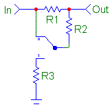
The staged attenuator circuit relies on the property that the attenuation of one stage does not depend upon the attenuation of the other stages. This is accomplished by designing the stages in such a way that their output resistance is independent on their switch position.

Lets design a single stage of an attenuator, around one switch:

Source resistance Rin = R1 =
Output resistance Rout = R2 =
Attenuation (switch=1) [dB] R3 =

You should specify an Rout larger than or equal to Rin!
If switch=0 then the stage attenuation is 0[dB].

In practice you would probably like to use Rin=0 (denoting an ideal source driving the first stage) or Rin=Rout (not spoiling resistance between the stages). In these cases one of the resistors will get a 0 value, resulting in a stage with 2 resistors around one switch.


Jos van Eijndhoven, January 2004,
Back to the Switch-Resistor page, Back to my home page