RelaiXedSMD -- DIY balanced pre-amplifier

Introduction
The Relaixed2 is an audio pre-amplifier design, created for easy re-builing by DIY audio enthousiasts.
This page describes its SMD version, which is a more compact implementation as result of selecting mostly SMD-type components.
The more compact implementation can free-up cabinet space for integration with a power amplifier.
Similar to its standard implementation, it targets the high-end audio segment. It is characterized by:
- The design provides a balanced (XLR) stereo output, and 6 selectable inputs
of which 2 are balanced inputs and 4 are single-ended (cinch/RCA) inputs.
Balanced cabling towards the power amplifier in principle provides cleaner audio signal transfer.
-
Audio volume control and stereo balance control is implemented through a series of relays, 6 per channel,
providing 1dB volume steps with high quality and reliability, beyond what can be obtained with other types of volume controllers.
-
Besides through a single front knob, the pre-amplifier can be remotely controlled through IR signals.
It supports multiple IR protocols, to provide large freedom in remote controller selection.
-
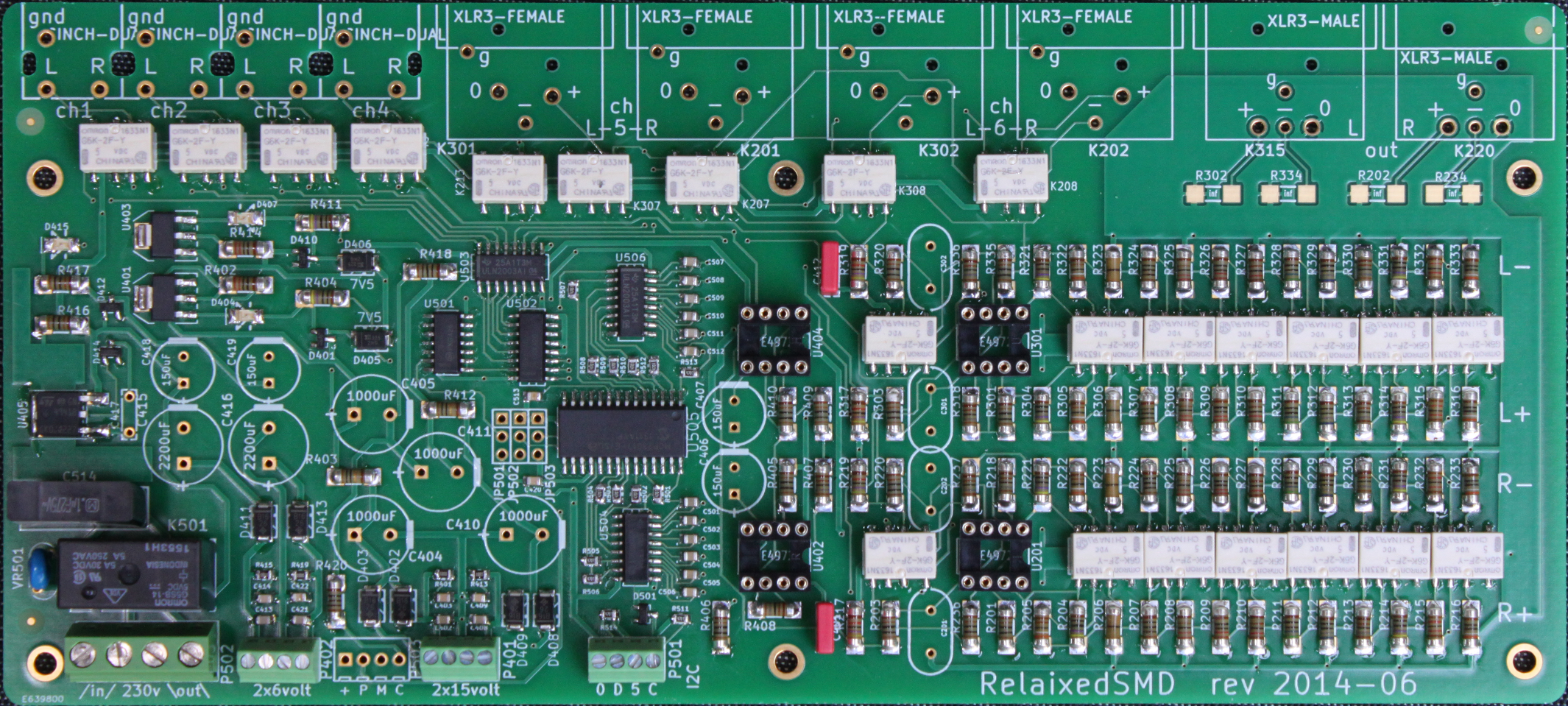
The hardware design entails one PCB containing the audio processing, the power supplies, some digital decoding,
and on-board audio connectors, and is to be placed against the back-plate of the pre-amplifier chassis.
Next to that, a small front-PCB contains a microcontroller, a 2-digit LED display, and the IR receiver,
and is to be located against the front-plate of the pre-amplifier.
-
The software ('firmware') of the embedded microcontroller can be easily updated through a USB connector.
All embedded software as well as the PC interface software is made public available in binary and source format.
-
Upon request I provide the PCBs to other audio hobbyists, as well as the required pre-programmed microcontroller.
These PCBs are being made with first-grade industrial quality, two-layer through-hole, and gold finishing,
which makes them very easy and robust for manual soldering.
For all other components I provide a component table with order-numbers for easy ordering at an online shop.
Note that I will not freely provide the PCB design files.
The RelaiXedSMD design shares with the RelaiXed2 design a special relay driving scheme that supresses audible glitches in the audio outputs that were experienced in other/earlier relay-based designs.
New in comparison with the earlier RelaiXed PCB design is the option to mount a PCB-based cinch-connector block,
as alternative to the more elaborate wiring of individual panel-mounted cinch connectors.
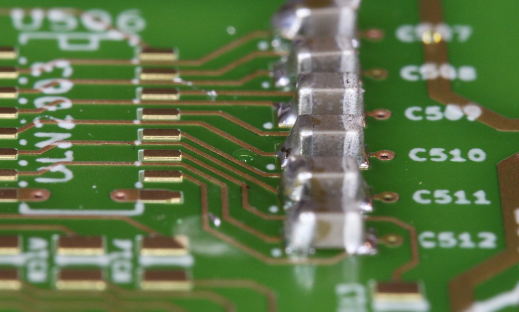
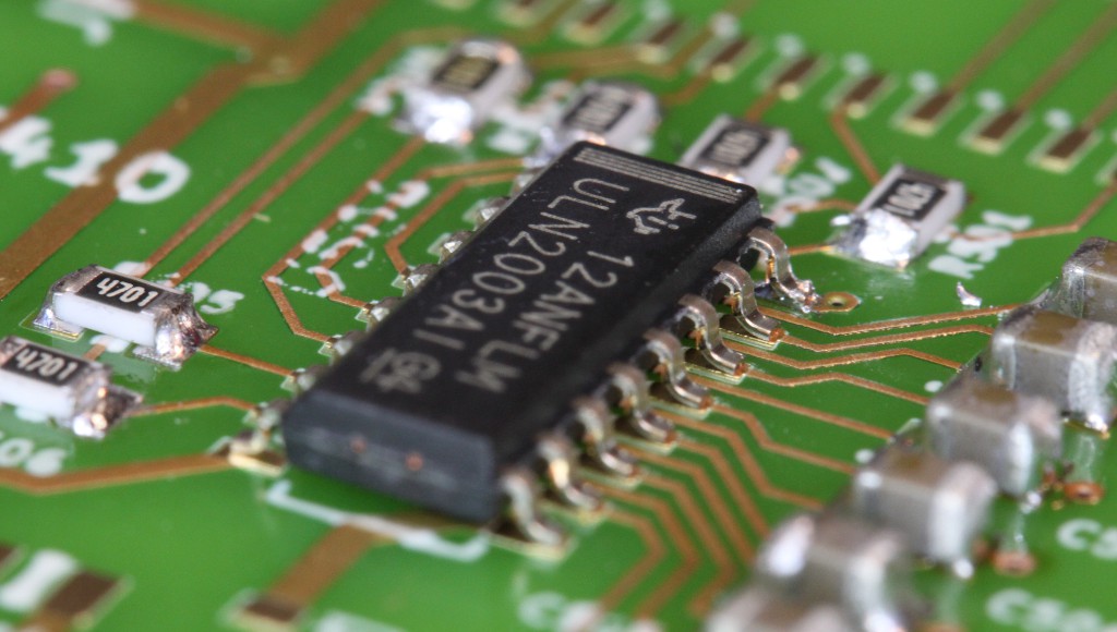
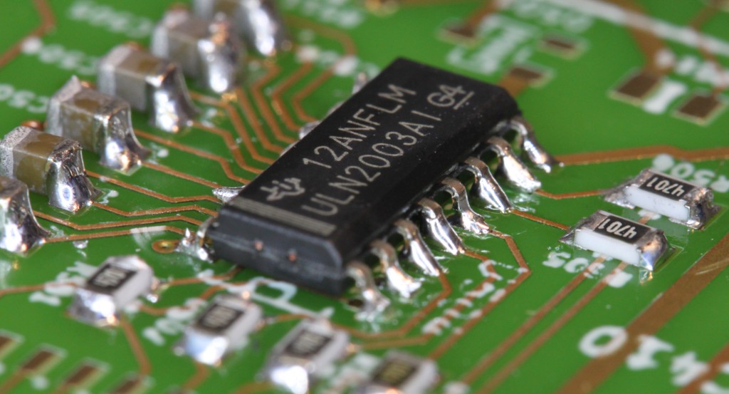
This is a foto of the volume control with the resistors and relays:
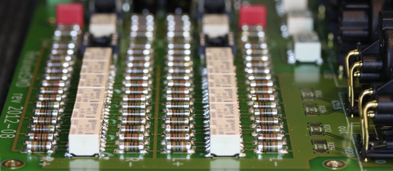
A chain of 6 relays provides 64 volume positions with steps of 1dB.
The separate attenuator relays for the left and right channels also provide balance control.
Design information
This SMD design is documented here with a couple of on-line documents and fotos.
The
user manual of the original RelaiXed2 is not yet cloned and adapted for this design, but is still usefull for background info.
-
The hardware design files with schematics and PCB layout with sizes: The new
SMDrelayPCB-20130224.pdf.
which used together with the original
FrontPCB-201108.pdf.
-
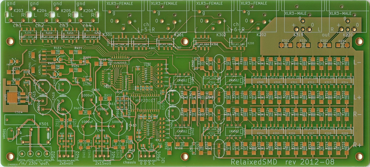
Picture of the produced PCBs, first prototype version, from my flatbed scanner:
SMD Relay-PCB top view
-
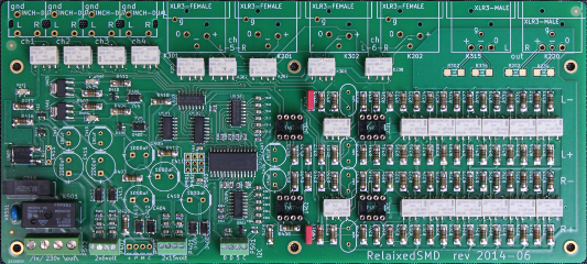
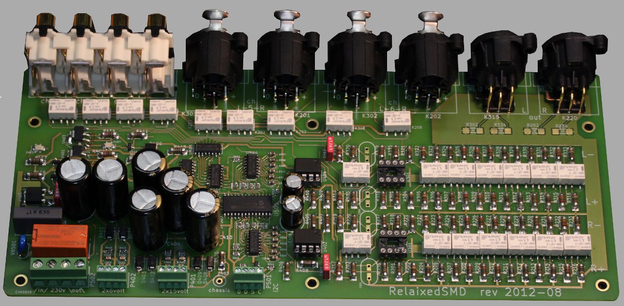
Foto of the board with mounted components. Note the mounted cinch connector block:
mounted PCB
-
Component list and prices
Online list at Octoparts.
The Octopart table allows you to create a shopping cart with a single click.
The actual component selection was tuned for 100% availability at Mouser:
for many components proper replacements would be available at the other shops.
Note that these online prices as quoted by Octopart are somewhat optimistic:
they quote USA prices, but in Europe the Mouser prices are somewhat higher, also sales tax still needs to be added.
Here is still my older list (not kept up to date anymore) which at the bottom shows some options for
components that are not mounted on the PCB, but are potenbtially interesting to complete your amplifier project:
Earlier omponent table.
-
The SW Design manual explaining the organization of and build process for the embedded software as well as for the PC-side interface software, is shared with the RelaiXed2 design: the software is identical.
-
The online software project,
that provides all source code in a revision control system (svn),
also in a web-browsable format.
If you want to contribute to improving/extending this software, please conact me.
PCB and microcontroller availability
PCBs are out of stock since 2018, not made anymore (by me)
The PCB availability as mentioned in the paragraphs below is NOT valid anymore!
Basically because I currently lack time for this project...
For any DIY audio hobbyist who wants to build this design and have PCBs fabricated,
the Gerber PCB design files are provided in
this zip archive.
NEW:
If you want to make your own modifications to the schematics or PCB,
I hereby provide the complete design source archive,
refreshed for use in KiCad version 5!
A pair of PCBs now costs €62,=.
The preprogrammed PIC18F24J50-I/P microcontroller costs €8,=.
Packaging and mailing with a 'sign-on-receipt' service costs €13,= throughout Europe, and €18,= elsewhere.
If you order more then one unit, I can offer 30% reduction on the price for the extra (2nd and further) units.
I do not send out sets of components: you better order these directly from an online shop.
A complete set of components costs roughly €200,=.
You might contact me for availability and price of a pre-built module, which I could have available sometimes.
Design background
Obviously, this single page is not suited to explain all of the design background.
Nevertheless I would like to mention some of my ideas that guided this design.
In the past I did design and listening tests on vacuum tube amplifiers.
That background and experience did lead me to:
- Do not use more semiconductors in the audio path then needed.
More semiconductors easily make the sound less open and transparent.
-
For those semiconductors that remain, use quality types that are designed for high bandwidth.
I suspect the non-linear (parasitic) capacitances inside the semiconductors. In devices that
support high-frequency operation these capacitances have lower (less disturbing) values.
Otherwise, the nonlinearity of these capacitances can be reduced by operating the design
at relatively high supply voltages.
-
Always choose good quality components!
Nevertheless, I often find the advertised/dedicated 'high end audio' components over-priced,
and instead look for first-grade professional (industrial) types.
In general it is good to look for low-noise components. Low noise often correlates with good production quality.
The resistor type and brand in this design is chosen for its excellent noise specification of 0.01uV/Volt,
at a very afforable price (compared 'high end audio' resistors).
Next to semiconductors, also capacitors are 'dangerous' in the audio path.
The only capacitors in this design on the audio signal path serve to decouple/eliminate high-frequency
input signal components (frequencies above 100kHz). These are small capacitors for which really good dielectric types
should be selected. In the top-view foto below one can distinguish the silver mica capacitors.
-
The relais + resistor attenuator avoids the weak contacts of a sliding potentio-meter,
and avoids the single-chip digital controlled integrated attenuators (as I distrust most semiconductors).
The attenuator in this SMD design was slightly updated to also allow a passive preamp with a higher-resistance attenuator.
To do this, you would need to adepts the attenuator resistor values with the help of my
online attenuator calculator.
-
The on-board XLR (and now also cinch) connectors provide a short and good-quality connection to the audio electronics,
without you having to worry about wiring audio inside your chassis.
(Although separate cinch connectors still do bring a quality advantage.)
No audio signals are routed to the front (display) module.
The digital electronics on the main (relay-) PCB are 'silent' during normal use: the digital signals do not
switch state, there is not a 'life' clock signal. This prevents interference from the digital side into
your precious analog audio signals. Only during volume- or channel-changes there is a moment of digital activity.
The digital circuit is strongly separated from the audio, there is not even a common ground signal.
-
The front-panel controls the main audio/relay board through an industry-standard I2C serial protocol.
This means that you could also create your own preamp control through other industry/hobby control boards and projects.
-
Good-quality components and tools lead to more satisfaction in this nice hobby
and to reliable devices with a long lifetime expectation. There is already too much rubbish being made...
One final warning: when turning the volume, one can clearly hear the mechanical clicking sound of the relays. If that would really
disturb you, relay-based attenuators are not your thing...
The audio opamp selection
Although this RelaiXed-SMD design mostly relies on compact SMD components, conventional DIL-8 sockets are used for its main audio opamps.
This allows for a wide selection of available (dual-) opamps, and an easy swap if you want to do a later upgrade or just test some alternatives.
The internet is full of stories on good audio opamps.
Be aware that, first, there is not just a good (or best) opamp: the suitability of a specific opamp highly depends on the surrounding circuit.
And, second, modern audio opamps tend to develop in the direction of low noise and low distortion, but definitely also towards a very high bandwidth.
Since I personally distrust semiconductors in audio for their non-linear (parasitic) capacitances, high bandwidth seems a promising direction for me...
-
The standard type listed for this amplifier is the LME49720.
This is in general one of the finest modern audio opamps available. Its basic version in a plastic DIL-8 package
is the default in above component list, and fits directly in this design.
-
However, for best audio performance,
I can advise its version in a TO-99 metal-can package: that one is somewhat more expensive, and provides an audibly more transparent sound.
Yes, that is somehow incredible, as its technical specs remain identical: it is really only a package change.
Unfortunately, the TO-99 metal-can package gets rather hot, and needs a little (TO-5) cooling fin.
This metal-can version -in my experience- does away with many sound problems that people often affiliate with opamps.
Although you can plug the wires of the TO-99 package directly in a DIL-8 socket, a
converter adapter is a more sturdy solution.
-
New update: recent experiments showed that the OPA1642
also behaves very good in this design, with a slightly more smooth and warm sound. This opamp is only available in a smaller SOIC package,
so you would need a tiny
adapter-board to mount it.
The circuit uses 4 such dual opamps: one each for left and right audio, where each half of the dual opamp is used for the + and - signal of the balanced audio,
and one each for the positive and negative power supply stabilization, where the halves are used for independent left and right channel voltage stabilization.
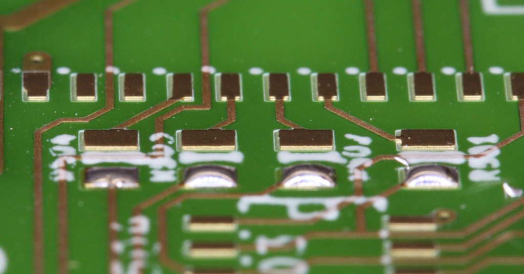
Mounting SMD components
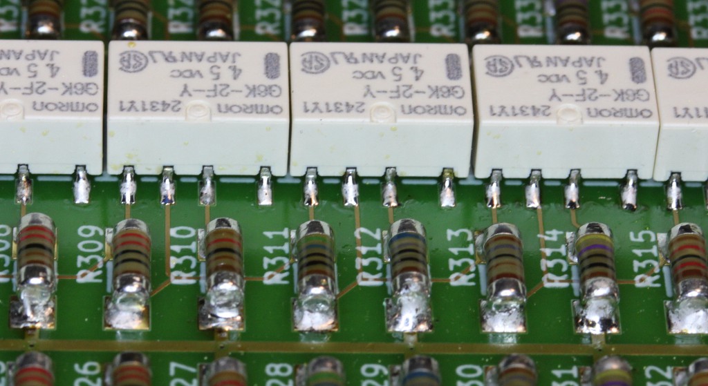
Mounting the components on this board is best done in an order with the lowest-profile components first.
That way, best accessibility for soldering is maintained.
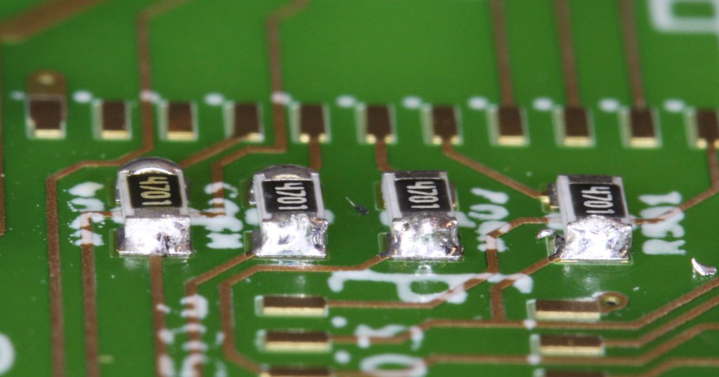
For manual soldering of these small SMD components, there is a standard procedure:
-
Use a soldering iron with a narrow-pointed tip, and thin soldering wire. A soldering wire thickness of 0.75mm to 0.5mm works fine for me.
-
Apply a little drop of solder on the pad of a single pin. Do this quickly, such that not all of the rosin flux in the solder already evaporates.
You can easily do this for several (many) components up front.
-
Hold the component in place, with a tweezers, and with your other hand heat-up the solder-drop under one pin. Take the soldering iron away, gently push the component down for flat mounting on the PCB surface.
-
Now solder the other pins, do not apply too much solder: regularly clean you solder-tip from excess solder.
Maybe re-do the first pin.
-
For the ICs with a row of nearby pins, you might accidentilly end up with a small drop of solder that spans the space between two neighbouring pins.
Do not worry about that, first just finish doing all its pins. Afterwards you can use 'solder wick (also called 'de-soldering braid') to remove such excess solder.
-
These are a few pictures from such soldering (click for a larger view):
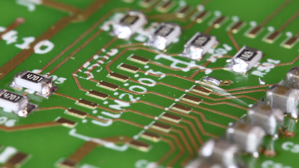
The picture below shows the PCB with lowest profile (mounted first) components.
It also shows the 4 sockets for the 4 dual opamps: 2 for the power supplies and 2 for the audio itself.
The photo might help you with your own assembly: Click for a real hi-res picture!
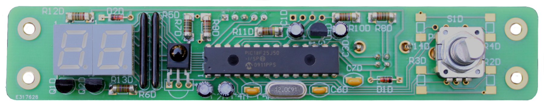
Front control module
Next to the main (audio and powersupply) PCB of above photo, the design uses a small front-side PCB with 2-digit display, the infrared receiver, and the user control knob. This PCB also contains the microcontroller for the digital control of the main PCB. These PCBs are connected through 4 wires. Obviously, audio signals are not passed to this front PCB. This PCB is actually identical to the one used for the 'classic'(non-SMD) version of the Relaixed, so it uses mostly through-hole components. This board also holds a USB connector which can be used to upload new firmware into the microcontroller. That connector is located on the back side and not visible on this photo:
Electrical specifications
| Bandwidth: |
DC - 330kHz (limited by input filter) |
| Signal gain at max. volume, cinch in to balanced out: |
1 : 1.55 + 1.55 (is +9.8dB) |
| Signal gain at max. volume, balanced in to balanced out: |
1 + 1 : 2.1 + 2.1 (is +6.5dB) |
| Signal input impedance: |
47 Kohm |
| Signal output impedance: |
400 Ohm |
| Distortion (1 kHz, 5V in/out, single-ended or balanced): |
0.0001% |
| Output noise density at max. volume, shorted input: |
-160 dBV/sqrt(Hz) is 10nV/sqrt(Hz) |
| Output signal/noise ratio in 20kHz audio band, relative to 2Vrms nominal signal: |
-123 dB |
| Left-Right channel separation at 1 kHz: |
-137 dB |
| Power consumption during standby: |
0.6 W |
| Power consumption at max volume: |
9 W |
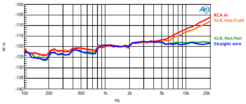
Distortion measurements, while using a LME49720 opamp, show extremely low values.
This indicates that -next to the opamps- also the other circuit components (resistors, capacitors, wiring) behave good.
Around 1kHz, -120dB corresponds to 0.0001% distortion, and is close to the 'straight wire' reference measurement.
Above 5kHz the distortion increases normally, except that in true balanced operation a cancelling occurs to maintain a very low distortion level.
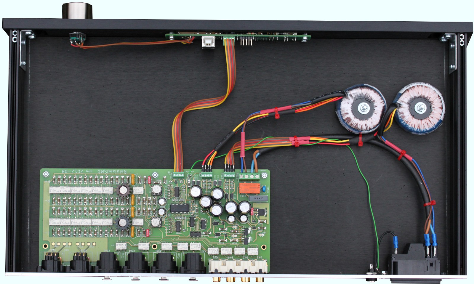
Building the relaixedSMD into a cabinet
I built my prototype into the same Hifi2000
slimline cabinet
as was done for the earlier
RelaiXed2 cabinet.
Note the shiny metal-can opamps in line with the relays, with a attached black ribbon cooling fin.

The audio connectors in default backpanel. This panel is made by
Schaeffer
from this design file:
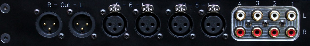
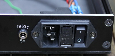
The chosen power-entry has both a power-switch and a fuse. The RelaiXed is normally not powered-off: in standby it can be powered-up through the remote control.
Thanks for your interest,
Jos van Eijndhoven
Sept. 28, 2019